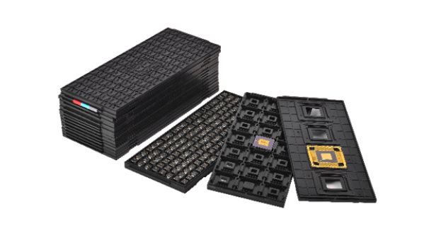
I. What is an IC Tray?
IC trays, also known as electronic chip trays, are plastic packaging trays custom-made for chips (ICs) by semiconductor packaging and testing companies. They are used throughout the entire process of chip packaging, testing, transportation, and storage, serving as core auxiliary components to ensure chip safety and production efficiency. Unlike ordinary packaging, IC trays must be precisely matched to chip sizes and packaging forms, acting as a key link between chip manufacturing and downstream assembly.
II. Core Uses of IC Trays: Dual Protection and Efficiency
The value of IC trays lies in two core dimensions: "protection" and "automation compatibility," covering diverse application scenarios:
- Anti-static protection: Prevents chip damage from electrostatic contact. Chips (especially MOSFETs and sensors) are extremely sensitive to static electricity, so IC trays block electrostatic conduction through material modification, reducing scrap risks.
- Physical protection: Shields chips from bumps, scratches during transportation and storage, while isolating dust and impurities to ensure chip yield.
- Automation compatibility: The standardized cavity design of IC trays enables precise chip positioning, adapting to automated testing equipment (e.g., visual inspection, probe testing) in packaging plants and robotic gripping on downstream assembly lines, significantly improving production efficiency.
In terms of packaging types, their compatibility is extensive, covering almost all mainstream chip packaging forms such as BGA (Ball Grid Array, used for high-end CPUs/GPUs), QFN (Quad Flat No-lead, used for automotive chips), QFP (Quad Flat Package, used for industrial control chips), as well as PGA, TSOP, TQFP, LQFP, PLCC, SoC (System on Chip), and SiP (System in Package).
III. JEDEC Standards: The "Universal Language" for IC Trays
Currently, the design of IC trays in the global semiconductor industry adheres to industrial standards set by the Joint Electron Device Engineering Council (JEDEC). As a recognized core standards organization in the global semiconductor field, JEDEC’s specifications ensure compatibility between trays, chips, and equipment from different manufacturers.
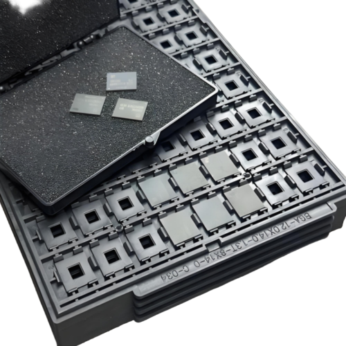
The core of this standard is "cavity matrix standardization": it clearly defines the cavity distribution and quantity of IC trays corresponding to chip sizes ranging from 3×3mm (micro sensor chips) to 22×22mm (large power chips). For example, small 3×3mm chips often use trays with a 20×20 cavity matrix (400 cavities total), while large 22×22mm chips typically use a 10×10 matrix (100 cavities total)—balancing space utilization and preventing chip extrusion.
IV. 5 Key Material Requirements for IC Trays
IC tray materials must balance protection, stability, and practicality, with 5 core requirements:
- Anti-static performance: Modified by adding antistatic agents, conductive carbon black, or conductive carbon fibers. Requirements vary by scenario: general industrial chips need a surface resistance of 10⁹-10¹¹Ω, while high-end sensitive chips (e.g., AI chips) require 10⁶-10⁸Ω to eliminate electrostatic breakdown risks.
- Temperature resistance: Chips need baking to remove moisture before terminal assembly (to avoid the "popcorn effect" during soldering). Baking temperatures are usually 125℃-150℃, and some high-reliability chips require short-term baking at 180℃. IC tray materials must be free of deformation, precipitation, and embrittlement at these temperatures.
- Dimensional stability: The gap between upper and lower IC tray layers must precisely clamp chip pins to prevent pin bending/breaking. Therefore, the warpage of materials after molding must be controlled within 0.3mm, and the dimensional change rate after long-term use must be ≤0.2%.
- Low water absorption: Humid environments can cause tray deformation and chip moisture damage. The 24-hour water absorption rate of materials must be ≤0.2%. Especially in rainy areas or high-humidity workshops, low water absorption avoids reduced positioning accuracy.
- Recyclability: To reduce costs and environmental pressure, materials must support recycling—e.g., PS and PP can be crushed and reshaped, while PET can be chemically depolymerized for regeneration, aligning with the semiconductor industry’s green production trends.
V. Common Material Classifications and Applications of IC Trays
IC trays are mainly made of conductive plastics through processes such as injection molding, baking, water washing, inspection, and packaging. Different materials are suitable for different scenarios:
- Polysulfone (PSU): Long-term temperature resistance above 150℃, high impact resistance, used for high-end automotive electronics and aerospace-grade chip trays (e.g., SiP packaged chips).
- Polyphenylene Ether (PPE): Balances temperature resistance and insulation, with good toughness, suitable for QFP and LQFP packaged chip trays prone to bumps.
- Polyetherimide (PEI): Temperature resistance up to 180℃, chemical corrosion resistance, used for high-reliability chips requiring high-temperature baking (e.g., industrial control MCUs).
- Acrylonitrile-Butadiene-Styrene copolymer (ABS): Low cost and good processability, used for TSOP and PLCC packaged chip trays in consumer electronics.
- Polyarylsulfide (PAS): Wear-resistant and oil-resistant, used for industrial-grade chip trays (e.g., power semiconductors) with frequent pick-and-place operations.
- Polypropylene (PP): Excellent toughness and light weight, suitable for temporary storage or short-distance transportation of chip trays.
- Polystyrene (PS): Cost-effective, used for low-demand consumer chip trays (e.g., ordinary sensors).
- Polycarbonate (PC): Good transparency and impact resistance, facilitating chip identification by visual inspection equipment, often used for BGA and QFN packaged trays.
- Polyamide (PA): Wear-resistant and aging-resistant, used for long-term recycled SiP and SoC packaged chip trays.
- Polymethyl Methacrylate (PMMA, Acrylic): Extremely high transparency, allowing visual inspection of chip status, used for high-end chip trays requiring visual checks.
- Polyethylene Terephthalate (PET): Lightweight and high-strength, suitable for large-batch long-distance transportation of BGA and TQFP packaged trays.
Among these, PMMA, PC, and PET are the mainstream materials in the market, accounting for over 70% of total usage. They balance performance and cost, meeting the needs of most consumer electronics and automotive electronics chips.
VI. 6 Key Specification Requirements for IC Trays (JEDEC Implementation Details)
To ensure compatibility and safety, IC tray design must meet strict specifications, with core clauses as follows:
6.1 Basic dimensions and tolerances: The minimum area of the vacuum suction zone must be ≥28mm² (to ensure stable adsorption by automated suction cups and prevent falling during handling); the total thickness of standard trays is 7.62mm (X.XX-type dimension) with a tolerance of ±0.13mm; for partial structural dimensions (e.g., cavity depth, protrusion height), X.X-type dimensions (e.g., 2.0mm) have a tolerance of ±0.25mm, and X.XX-type dimensions (e.g., 2.00mm) have a tolerance of ±0.13mm.
6.2 Design approval and simulation: IC tray design must refer to the POD (Product Specification Document) of the corresponding chip, and be jointly approved by the supplier’s engineering department (structural verification) and quality department (compliance review); the simulation report must include chip drop, vibration, and temperature cycle tests to ensure no chip offset or damage in the tray, and the tray gap must not be ≥2x the chip thickness (to avoid chip shaking).
6.3 Temperature resistance and mechanical tests: Must pass continuous baking at 150℃ (duration refers to JEDEC standards for corresponding products, mostly 24 hours). After testing, the tray must be free of chips, cracks, or breaks; the bending test must withstand ≥10kg of force for 30 seconds without breaking; the strapping test (trays stacked in "1+1" and "10+1" modes) must withstand 23±2kg of tension without strapping slippage or tray damage.
6.4 Stacking gap control: When stacking trays of the same batch, the gap between two layers must not exceed 0.5mm—excessive looseness causes transportation shaking, while excessive tightness makes separation difficult, affecting automated pick-and-place efficiency.
6.5 Resistance consistency: Tested in accordance with JEDEC JESD22-A114 standards, the surface resistance of the tray must be uniformly distributed without local deviations (e.g., resistance difference between edge and center ≤1 order of magnitude) to ensure consistent anti-static effects across the entire area.
6.6 Detailed design requirements:
- 3 strapping grooves must be set (1 on each side and 1 in the middle, with uniform spacing to adapt to automated strapping machine positioning);
- The side must be marked with drawing number, version, and production date (font height ≥2mm, clearly legible);
- The tray ears must be marked with applicable chip size (e.g., "10×10mm BGA"), type, tray cavity quantity (e.g., "16×16=256Pcs"), material, temperature resistance mark (e.g., "Tmax 150℃"), recycling mark, and lead-free mark;
- A reverse foolproof design is required (e.g., one side of the tray ear is convex and the other is concave; convex parts collide and cannot fit when stacked in reverse, or the gap >2mm);
- Cavity enclosures must be reinforced with ribs (width ≥1mm, spacing ≤5mm to prevent enclosure deformation) and have an Interlock design (adjacent trays engage with each other when stacked to improve stability);
- The overall thickness distribution is uniformly "2.00mm (cavity protrusion height) + 5.62mm (base thickness) = 7.62mm"—an industry universal dimension;
- The priority order for cavity side design: beveled bearing type (40°-50°, facilitating chip insertion) > substrate bearing type (suitable for leadless chips) > spherical bearing type (reducing chip scratches).
ICgoodFind’s Perspective
ICgoodFind is deeply rooted in the semiconductor supply chain and understands the importance of IC trays for chip production safety and efficiency. Relying on cooperation with high-quality tray manufacturers, we can provide customers with IC trays that comply with JEDEC standards and are compatible with multi-package types such as BGA/QFN/SoC, covering consumer electronics, automotive electronics, and industrial control fields. We also offer IC tray selection consulting to help customers avoid risks such as improper materials and mismatched dimensions, ensuring the full-process safety of chips and improving supply chain collaboration efficiency.
